• Zum Inhalt springen
  • Zur Seitenspalte springen

Technik News

Das Blog zu IT, Mobilfunk & Internet

Reviews

Autopsy of a Logitech MX5000, and the reason why it sucks

März 14, 2007 von Harald Puhl

I wrote before about the Logitech MX5000 Bluetooth keyboard & mouse combo, and there are plenty of posts around the web that confirm that the product sucks – badly.

To recap a bit, the problems are random reboots of the keyboard, disconnections of keyboard and mouse, erratic mouse behavior (including spontaneous motion of the cursor), and repeated keystrokes after the keyboard has not been used for a few minutes (resulting in things like “aaaaaaaafter the news…”). In all, a very frustrating and annoying experience, for a rather expensive combo. Logitech seem to acknowledge the problem, but I have not yet seen any form of update that could fix this, and my theory is that the problem cannot be fixed with a simple software update.

Declaring the keyboard and mouse defunct, I performed an autopsy, which revealed a few interesting facts (details after the jump):

  • The Bluetooth dongle has a very very strange RF design – it uses a normal groundplane meander PCB antenna, but then it has a copper-wire loop antenna on top.
  • Dongle and keyboard use Bluetooth chipsets from different manufacturers (CSR and Broadcom), in theory interoperable, in reality…well.
  • The touchpad uses a very crappy sensor design, which explains the lack of responsiveness and uselesness of the scrolling controls.

Let’s start with the dongle. Below are a couple of photos of the opened device, the first with the loop antenna in place, the second with it removed, showing the meander. If someone with better RF knowledge than me can explain why this makes sense, I would be grateful. The design of the loop itself is wrong for 2.4GHz, having a wire length about 10 times larger than what would be required given its size.

dsc_1279dsc_1280.jpg

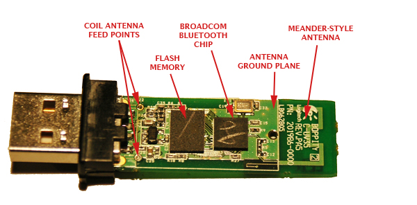
The dongle uses a Broadcom BCM2045 chipset, with a 4Mbit flash memory onto which the firmware is loaded. The meander is a PCB track designed for 50ohm impedance, coupled to the chipset via a normal inductor-resistor-inductor matching network. Noticeable is the lack of baluns or filters, I’ll have to check the datasheet (if it’s publicly available) on this aspect.

Let’s take a look at the keyboard, starting with the touch controls. These are built into the keyboard as a separate module, linked to the main control board with a flat ribbon cable, and consist of three main pieces – the PCB and touch sensors, external case with printed cover, and a plastic support with built-in LED light pipes. The controls are made with a layer of gold-plated copper, printed on the underside of the PCB, and on the top side lives the control chip, made by Synaptics (who also makes touchpad systems and other stuff).
dsc_1289.jpg

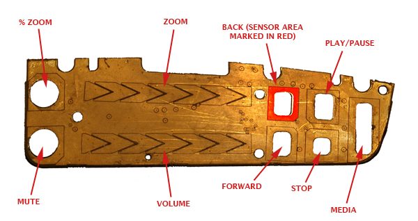
The principle by which these type of controls work is capacitance changes. When you place your finger near the sensor, a capacitive effect takes place (using the air and any other material in between as dielectric), which can be measured. It is very small, but enough to give an indication that a finger is present. There are a few rules that one must follow when designing such touchpads, as any interference in the capacitive effect can have negative results on the ‘feeling’ of the controls. Namely, ground planes have to be carefully controlled, and usually placed away from the sensor area, the sensors have to have a minimum size in order to be effective, and any trace routes from the sensor pad to the control IC have to be kept tight, avoiding cross-overs and other disturbances.

I am not familiar with the Synaptics chip, but I have worked with Quantum Research QProx devices, and I cannot see how the physics of capacitance could be avoided in either case. The MX5000 design violates all these rules. The sensor areas are irregular, with a gaping hole in the middle to allow for LED light to pass through, there are ground planes all over the PCB, the tracks meet and part at various spacings and passing right next to ground planes. The biggest joke seems to be the ’sliding’ sensors for the volume and zoom. These are depicted on the face of the keyboard as smooth analog paths, as if one could go from minimum zoom or volume to maximum by sliding the finger to each end of the vertical scale. The truth is that to change the volume in any significant way, one has to repeatedly slide the finger along the whole path of the scale several times, and in some cases, the detection doesn’t work. You end up looking demented, rubbing away the side of your keyboard repeatedly! As is shown on the photo, the sliding scale has only 7 distinct sensors, thus giving you a maximum of six detectable steps in either direction (each step is signaled by the triggering of one sensor, then the one adjacent, determining direction of finger travel). It would be a bad idea to place the whole volume or zoom range on a scale of six steps, and so they settled for the crazy-monkey-rubbing-keyboard action instead.

The next two pictures show the PCB inside the plastic assembly that houses the faceplate. Notice how the cutouts allow for light from the LEDs to be piped towards the labels and icons.

dsc_1292

dsc_1294

And finally, the last part of the broken equation – the Bluetooth module on the keyboard. It uses a CSR BlueCore3 ROM, which is cheap but cannot have its firmware modified after the die has been printed, meaning whatever bugs you had in the device will be there forever. Again, the module uses a meander antenna. Now, I am not too familiar with the Broadcom chipset, but I have worked with CSR chipsets quite a bit, and know they provide a balanced antenna output, this means that to use an antenna such as a meander or chip, you have to go through a balun. I don’t see a balun on the MX5000’s module, and so it appears they have attempted to balance the antenna with another set of meanders, which can be seen between the chip and the large main meander in the picture below:

dsc_1296

Again, this design doesn’t seem to be the best in terms of RF performance, specially when you have a large inductor nearby (L1).

Conclusion? Don’t buy one of these, if you want to go wireless, get one of the non-Bluetooth (some also work at 2.4GHz) keyboard/mouse combinations, and I would still say get a Logitech, as they make some very good ones, such as the MX3000. I’ve always used Logitech, but the MX5000 has been a real lemon.

How not to install a WiFi antenna

Dezember 25, 2006 von Harald Puhl

Leaving aside regulatory issues that may turn this particular setup into an illegal operation, I will better not describe the quality of the installation to be polite. Check out this picture:

wifi antenna

Spotted the problem yet? Radio antennas are affected by any element that is present around them, even non-metallic elements, such as the ground. In this particular case, kanijo, a Fonero, has attempted to provide more “range” to his FON hotspot, which is in itself commendable, however, the means may not result in the desired end.

You can see that the vertical omni antenna, a carefully tuned radiating element, has been strapped to a metallic pole, which also runs a coaxial cable into a TV antenna right on top. The router is inside a sealed plastic box, with power and Ethernet going into it from below. There is no way that this antenna is radiating correctly, as the pole that supports it is probably grounded (if it has been installed according to regulations), and even if it is not, it is inducing an imbalance into the tuned element, causing a large amount of RF to be attenuated. The user reports good results with it, which are most likely due to good luck.

The second problem with this type of setup is that vertical antennas don’t emit downwards, and thus will provide very limited coverage to users below the antenna. There is some downwards bleed of course, but it will only reach lower users that are some distance away from the antenna.

Recommendations for these sort of setups: install the antenna right at the top of its own pole, and ground the pole. If you have no choice but to use an existing pole, get a T arm fitting and mount the antenna at least 1 meter (3 feet) away from the pole. A perfect example of such as setup, in this case with two supports as the antenna is rather large and care for wind load is needed, is this (credit to Roger Halstead):

Check out Roger’s page, it is a very good read if you are interested in radio installations.

Vodafone HSDPA with the Huawei E220 USB modem

November 22, 2006 von Harald Puhl

Went to my local Vodafone store to pick up the new Huawei E220 HSDPA USB modem, which with a 49 Euro monthly contract gives you 1GB of transfer at 1Mbps maximum, and free mobile to fixed landline calls – pretty good deal if you ask me. For 59 Euro you get 5GB of transfer, at the full 3.8Mbps that HSDPA offers. These are theoretical rates, as they will depend on a number of factors, such as how many people are also using the same cell, your coverage and the quality of the link.
We can argue all we want about how convenient WiFi is, being omnipresent et al, but in reality, it’s rather hard to get connected while on the road. Let’s examine the following scenarios, and you tell me the chances of getting connected over WiFi:

  • Riding the train or bus home.
  • Getting a lift from a friend in his/her car.
  • Opening your laptop at a random location (cafeteria, bar, etc. that you haven’t before scouted for open WiFi).
  • On a plane, waiting for the next free takeoff slot that you hope the pilot won’t miss because he was checking the fatness of his wallet.

Let’s be honest – free open WiFi is great once you have identified the locations where you can get connected, such as a friend’s house or the local coffee shop. Other solid commercial alternatives make it easier to find WiFi, as they tend to be present at well-known locations. Walk into any Starbucks or hotel, and you’re bound to find at least for-pay wireless.
For me, on the 30 minutes to 1 hour it takes to get home on the train or bus, being able to get connected is great. The convenience of simply opening the Mac and getting online beats the guesswork of WiFi. I tried getting the Mac working with my Nokia N93 over Bluetooth, but it was just too unstable – one day it worked, the next simply refused to even connect. A more in-depth review of the device is coming, once I get a chance to roam about with it for a while.

So far, installation on the Mac was pretty straightforward, download the setup package from Vodafone’s site (they don’t tell you this in the manual), which then enables the modem as a networking device. If you don’t follow this step, it can get recognized as a storage device, which is not particularly useful for a modem. The one thing I don’t understand is why it comes with a miniUSB cable that ends in two USB connectors, my guess is it’s power-related (some USB ports don’t provide the full 500mA they are supposed to provide).

Autopsy of a Fonera

Oktober 6, 2006 von Harald Puhl

Yesterday, I posted a few pictures of the opened Fonera, with a few initial views on the device. When I tried to plug it in, it failed to work, only the power LED lighting up. Neither the WiFi signal was coming up, nor the ethernet port was tickling the switch.

The only course of action? To open it up even more. So, the aluminium chassis came off, and that’s when I realized I had seen this before. The WiFi section, which includes the Atheros AR2315, crystal, filters, power amplifiers and ancilliary circuitry are housed inside this casing, and correspond to a reference design provided most likely by Atheros themselves. Check out the Meraki Mini router. For reference, I provide a side-by-side picture below (click for large image).

Meraki Mini vs Fonera

There is nothing wrong with using reference designs per se, as it is the fastest and easiest way to bring a product to market. If you don’t need to customize your design much, simply use what the manufacturer suggests, and you will be playing on the safe side. A perfect example is Bluetooth headsets, where CSR dominates the market. Virtually all headsets in the market use their reference design, with very little changes between them, other than physical placement of LEDs and buttons.

Block-by-block, here is an overview of the Fonera.

Power

Power is supplied to the Fonera via jack SK1, and is fed through a rapid fuse (Polychem type) to a simple drop-down regulator, which drops voltage from around 5V (4.85V as measured on the wall power supply, using a Fluke 179 multimeter) to 3.3V. The regulator appears to be an AME1117 (though the package markings read AME117), in its CCCT configuration, TO-252 form factor. The regulator is stabilized using three electrolyic capacitors. In these types of regulators, ESR (equivalent series resistance) of the input decoupling capacitors is very important, and this can usually be controlled nicely with tantalum capacitors. These are very expensive compared to electrolytic, however.

There is a second stage of regulation, this time done by an Anpec APL1117, which further drops the voltage to 2.5V. This supply appears to be used by the wireless subsection. Two ceramic capacitors stabilize the regulator.

Without the Atheros chip in place, the PCB drew 90mA at 5V, or 450mW. Since the device was not functioning, the total supply current with WiFi active could not be determined.

Memory

Two memory ICs are available on the Fonera, the first is an ST M25P64 serial flash, with a 50MHz SPI bus and 64Mbit capacity (8MB), in 300mil SO16 format. The fact that SPI has been chosen has the advantage that extra memory devices could be attached to the bus, but it has the caveat that it is slower than a parallel bus. Thus, flashing a new firmware could take a rather long time. Interestingly, there are two footprints on the PCB, presumably to fit a different size and format memory IC, one SO16 and one SO8.
The second memory IC is a Hynix HY57V281620E synchronous DRAM, with a capacity of 128Mbit organized in 16bit blocks. In practice, this results in 16MB of RAM available to the processor.

Ethernet

At the heart of the wired ethernet subsystem is an Altima AC101 ethernet transceiver, capable of 10/100 full duplex operation. The IC is placed on the bottom layer of the PCB, and runs off a 25MHz crystal, strangely placed next to the main power regulator, where it could absorb electrical noise. Usually, crystals are placed well away from sources of interference. Nothing else too exciting here, the transceiver is connected to a standard RJ45 socket, TP1.

Wireless

The wireless section is the most interesting. This is where the Atheros AR2315 single-chip WiFi processor lives. Little public information is available about this or any other Atheros chipset, so it is hard to figure out exactly how it is put in place, but a few details are clear.

First, the chip gets hot. This is why a double heat-conductive adhesive tape bonds the surface to the metal cover, and in turn to the heatsink placed on top. The processor runs from a 40MHz clock source. After the Atheros core, come a couple of filters, and a power amplifier stage. This then runs off to the two antenna tracks. The first antenna exits the aluminium cage and runs up to a test connector. This connector breaks the antenna track when the right mating plug is inserted, which is then fed into a dedicated RF analyzer, which validates that the device is within constraints.

After the antenna test point, there is a split, which can be configured using a zero-ohm resistor, to run to an internal solder pad, or to a PCB-mounted right-angle SMA connector. It is unclear why they chose to use the solder pad, as an in-place soldered connector needs less handling than soldering a pigtail by hand. Besides, my intuition tells me the losses would be lower – I will test this when I get a working Fonera. Both tracks run through an impedance matching network, consisting of two capacitors to ground from the RF track, and an inductor between the capacitors . The purpose if this small circuit is to get the impedance of the PCB track as close to 50 ohms as possible. If the track impedance is mismatched to the antenna, losses take place.

The second antenna runs straight to a PCB pad, where a pigtail may be soldered, also passing a matching network. Below is a picture showing the details of this subsection.

Fonera - WiFi subsystem in detail

Interfaces

There are two IDC-style connectors on the PCB, one 2×5, and one 2×7 but unpopulated. The 2×5 looks like a serial connector, as only power, ground and two tracks lead out from it. The layout has to be studied in more detail to confirm this assumption.
It can be speculated that this is in fact a serial port, but without the AR2315 pinout, this cannot be determined for sure. The 2×7 header seems to be a JTAG interface, possibly compliant with MIPS EJTAG 2.6. The mapping of the header pins to the AR2315 BGA balls is shown below (thanks for adding a row/column silkscreen for the Atheros chip, and thanks to the OpenWRT project wiki for the JTAG information!):

Fonera - JTAG connector

Between the Ethernet jack and the empty SMA footprint, there is a footprint of 6-way header, which needs a bit more study to determine where it leads internally [I will update the post when I find out –Mike].

Conclusion

This is a very compact and simple WiFi router, designed not for being easy to hack, but for lowest cost. The cheap power regulator, use of large SMDs and choice of pigtail rather than board-mounted SMA connector point in this direction. There is only one port which could be used for something useful, if it is indeed a serial port, the only two GPIOs available being the WLAN and Ethernet LEDs – as long as the Ethernet LED is not controlled by the Altima but by the Atheros. The power LED is on as long as there is power applied to the device, so there is no control over this by the Atheros processor. Power consumption is a bit high, considering the wireless device was not present. The PCB layout is very professional, except in a few particular cases such as the large crystal, but overall, quite nice.

In all, a very small device which could have a lot of potential, had it not been for its lack of I/O. It is unclear whether the router will accept custom firmware, as there are rumors that an encryption & signature system is used. The Fonera is probably OK for regular use by Foneros, but it does not have the hackable edge of the Linksys WRT54Gx. The only suprise could come from the edge connector, as of yet of unknown usefulness.

References

Atheros AR2315 chipset website section and product brief.

The naked Fonera

Oktober 2, 2006 von Harald Puhl

After a few days of silence, digesting the hubbub created by my analysis of Fon’s status, I’ve put my head back into more useful things than answering hate mail and out-of-line comments (thanks to those who provided balanced views, either for or against!). So, I decided to open a Fonera and see what lives inside.

A full review is coming, but first impressions:

  • The plastic casing looks and feels very nice, the molds must have been expensive, as the different parts mate very well.
  • Inside lives a single PCB, with components on both sides. The top holds the bulkier components, such as power regulator, RAM and WiFi section, inside an aluminium RF shield.
  • The PCB looks professional and well laid out on first inspection.
  • Components used (I haven’t opened the aluminium chassis yet) are older SOIC and TSSOP, thus cheaper to handle and solder. Balled components require from special handling, such as baking in hydrogen for 24 hours to dry them before soldering, etc.

Here are some pics (click each photo for bigger views on Flickr) I have taken with a Nokia N93 (really nice phone btw, mini-review coming):

Fonera - underside of casing

The underside of the case, with screws off.

Fonera - perspective view

Perspective view of the top PCB.

Fonera - Bottom PCB

Bottom side of the PCB.

Fonera - firmware version

Sticker on the flash IC showing the firmware version.

AllPeers: Suckiness 2.0 (Beta)

September 4, 2006 von Franz Hieber

Finally, after months and months of hype and excitement, AllPeers launched. In Beta of course, lest it not be considered a Web 2.0 company.

Me and a friend installed the FireFox plugin, and fired it up. To start with, the buddy search mechanism is terrible. I actually typed my friend’s name, got a result, and added it to my roster – turns out it wasn’t even his profile. You cannot see details about the search results, which is a problem. With Skype, for example, sometimes you can turn up a dozen of hits on a buddy search, but at least you can get an idea of who is behind each result.

Once added a friend, it was time to share some files. I added a couple to my shared folder, and the files showed up there. My friend could not see them. I refreshed, and the files dissapeared. By the time I ended the test and decided to remove the plugin, I still hadn’t managed to get the files to stay put. My friend shared one file. It showed up twice on my screen (?!). The actual download of the file went well, but after that, the files also dissapeared from his screen.
There are a lot of bugs as it stands – at one stage, I had a buddy selected, but the screen showed “When ABC shares some files, you will see them here”, where ABC was my nickname. When I removed a buddy from my list, I could still see his shared files until I changed the folder view!
Frankly, platforms such as Pando work much better in terms of stability and ease of use. I am sure AllPeers will eventually iron out the issues, but right now, the service is a non-starter. This post also talks about the system being built upon a bug in FireFox, which when fixed will kill its ability to work as a P2P endpoint – any confirmation on this?

  • Seite 1
  • Seite 2
  • Nächste Seite aufrufen »

Seitenspalte

Tags

3D-Drucker Amazon AOL Apple asus memo pad Blackberry Dell DSL E-Book E-Book-Reader Ebay Elster Facebook Google Google Android Handy Hardware Hotmail IBM Internet Makerbot Microsoft mobiles Internet Netbook Prism Quantencomputer Rundfunkbeitrag Samsung samsung galaxy fame Samsung Galaxy Mega Samsung Galaxy Tab SchülerVZ Skype Smartphone Software sony xperia tablet z Suchmaschine Tablet Tintenpatronen Twitter Typo3 WebOS WhatsApp Xing Yahoo

Technik News Kategorien

Ausgewählte Artikel

LTE tilgt weiße Flecken und drückt aufs Tempo

LTE steht für Long Term Evolution und zugleich für den Vorstoß des mobilen Internets in die erste Liga der Breitband-Internetverbindungen. [...]. Heutige Angebote für mobiles Internet bringen 3,6 oder gar 7,2 MB/sec. Der Zugang erfolgt dabei meistens über einen Internet Stick der dank USB-Schnittstelle sowohl an einem Laptop wie auch am Desktop-Computer verwendet werden kann.


Externe Festplatte mit 3,5 Zoll, 2,5 Zoll oder 1,8 Zoll

Angeschlossen wird die externe Festplatte über USB, Firewire, eSATA oder einen Netzwerk-Anschluss. Vorsicht: Bei manch einer externen Festplatte stört ein lärmender Lüfter. Die kleineren Notebook-Festplatten sind 2,5-Zoll groß. Eine externe Festplatte mit 2,5-Zoll nimmt in den meisten Fällen über den USB-Anschluss Kontakt zum Computer auf und wird über dasselbe Kabel auch gleich mit Strom versorgt.

Inhaltsverzeichnis | Impressum und Datenschutzerklärung