Yesterday, I posted a few pictures of the opened Fonera, with a few initial views on the device. When I tried to plug it in, it failed to work, only the power LED lighting up. Neither the WiFi signal was coming up, nor the ethernet port was tickling the switch.
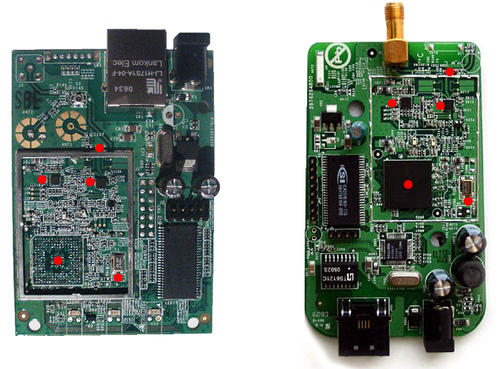
The only course of action? To open it up even more. So, the aluminium chassis came off, and that’s when I realized I had seen this before. The WiFi section, which includes the Atheros AR2315, crystal, filters, power amplifiers and ancilliary circuitry are housed inside this casing, and correspond to a reference design provided most likely by Atheros themselves. Check out the Meraki Mini router. For reference, I provide a side-by-side picture below (click for large image).

There is nothing wrong with using reference designs per se, as it is the fastest and easiest way to bring a product to market. If you don’t need to customize your design much, simply use what the manufacturer suggests, and you will be playing on the safe side. A perfect example is Bluetooth headsets, where CSR dominates the market. Virtually all headsets in the market use their reference design, with very little changes between them, other than physical placement of LEDs and buttons.
Block-by-block, here is an overview of the Fonera.
Power
Power is supplied to the Fonera via jack SK1, and is fed through a rapid fuse (Polychem type) to a simple drop-down regulator, which drops voltage from around 5V (4.85V as measured on the wall power supply, using a Fluke 179 multimeter) to 3.3V. The regulator appears to be an AME1117 (though the package markings read AME117), in its CCCT configuration, TO-252 form factor. The regulator is stabilized using three electrolyic capacitors. In these types of regulators, ESR (equivalent series resistance) of the input decoupling capacitors is very important, and this can usually be controlled nicely with tantalum capacitors. These are very expensive compared to electrolytic, however.
There is a second stage of regulation, this time done by an Anpec APL1117, which further drops the voltage to 2.5V. This supply appears to be used by the wireless subsection. Two ceramic capacitors stabilize the regulator.
Without the Atheros chip in place, the PCB drew 90mA at 5V, or 450mW. Since the device was not functioning, the total supply current with WiFi active could not be determined.
Memory
Two memory ICs are available on the Fonera, the first is an ST M25P64 serial flash, with a 50MHz SPI bus and 64Mbit capacity (8MB), in 300mil SO16 format. The fact that SPI has been chosen has the advantage that extra memory devices could be attached to the bus, but it has the caveat that it is slower than a parallel bus. Thus, flashing a new firmware could take a rather long time. Interestingly, there are two footprints on the PCB, presumably to fit a different size and format memory IC, one SO16 and one SO8.
The second memory IC is a Hynix HY57V281620E synchronous DRAM, with a capacity of 128Mbit organized in 16bit blocks. In practice, this results in 16MB of RAM available to the processor.
Ethernet
At the heart of the wired ethernet subsystem is an Altima AC101 ethernet transceiver, capable of 10/100 full duplex operation. The IC is placed on the bottom layer of the PCB, and runs off a 25MHz crystal, strangely placed next to the main power regulator, where it could absorb electrical noise. Usually, crystals are placed well away from sources of interference. Nothing else too exciting here, the transceiver is connected to a standard RJ45 socket, TP1.
Wireless
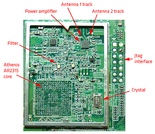
The wireless section is the most interesting. This is where the Atheros AR2315 single-chip WiFi processor lives. Little public information is available about this or any other Atheros chipset, so it is hard to figure out exactly how it is put in place, but a few details are clear.
First, the chip gets hot. This is why a double heat-conductive adhesive tape bonds the surface to the metal cover, and in turn to the heatsink placed on top. The processor runs from a 40MHz clock source. After the Atheros core, come a couple of filters, and a power amplifier stage. This then runs off to the two antenna tracks. The first antenna exits the aluminium cage and runs up to a test connector. This connector breaks the antenna track when the right mating plug is inserted, which is then fed into a dedicated RF analyzer, which validates that the device is within constraints.
After the antenna test point, there is a split, which can be configured using a zero-ohm resistor, to run to an internal solder pad, or to a PCB-mounted right-angle SMA connector. It is unclear why they chose to use the solder pad, as an in-place soldered connector needs less handling than soldering a pigtail by hand. Besides, my intuition tells me the losses would be lower – I will test this when I get a working Fonera. Both tracks run through an impedance matching network, consisting of two capacitors to ground from the RF track, and an inductor between the capacitors . The purpose if this small circuit is to get the impedance of the PCB track as close to 50 ohms as possible. If the track impedance is mismatched to the antenna, losses take place.
The second antenna runs straight to a PCB pad, where a pigtail may be soldered, also passing a matching network. Below is a picture showing the details of this subsection.

Interfaces
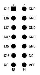
There are two IDC-style connectors on the PCB, one 2×5, and one 2×7 but unpopulated. The 2×5 looks like a serial connector, as only power, ground and two tracks lead out from it. The layout has to be studied in more detail to confirm this assumption.
It can be speculated that this is in fact a serial port, but without the AR2315 pinout, this cannot be determined for sure. The 2×7 header seems to be a JTAG interface, possibly compliant with MIPS EJTAG 2.6. The mapping of the header pins to the AR2315 BGA balls is shown below (thanks for adding a row/column silkscreen for the Atheros chip, and thanks to the OpenWRT project wiki for the JTAG information!):

Between the Ethernet jack and the empty SMA footprint, there is a footprint of 6-way header, which needs a bit more study to determine where it leads internally [I will update the post when I find out –Mike].
Conclusion
This is a very compact and simple WiFi router, designed not for being easy to hack, but for lowest cost. The cheap power regulator, use of large SMDs and choice of pigtail rather than board-mounted SMA connector point in this direction. There is only one port which could be used for something useful, if it is indeed a serial port, the only two GPIOs available being the WLAN and Ethernet LEDs – as long as the Ethernet LED is not controlled by the Altima but by the Atheros. The power LED is on as long as there is power applied to the device, so there is no control over this by the Atheros processor. Power consumption is a bit high, considering the wireless device was not present. The PCB layout is very professional, except in a few particular cases such as the large crystal, but overall, quite nice.
In all, a very small device which could have a lot of potential, had it not been for its lack of I/O. It is unclear whether the router will accept custom firmware, as there are rumors that an encryption & signature system is used. The Fonera is probably OK for regular use by Foneros, but it does not have the hackable edge of the Linksys WRT54Gx. The only suprise could come from the edge connector, as of yet of unknown usefulness.
References
Atheros AR2315 chipset website section and product brief.