After a few days of silence, digesting the hubbub created by my analysis of Fon’s status, I’ve put my head back into more useful things than answering hate mail and out-of-line comments (thanks to those who provided balanced views, either for or against!). So, I decided to open a Fonera and see what lives inside.
A full review is coming, but first impressions:
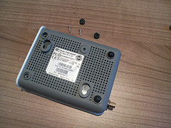
- The plastic casing looks and feels very nice, the molds must have been expensive, as the different parts mate very well.
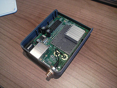
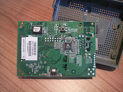
- Inside lives a single PCB, with components on both sides. The top holds the bulkier components, such as power regulator, RAM and WiFi section, inside an aluminium RF shield.
- The PCB looks professional and well laid out on first inspection.
- Components used (I haven’t opened the aluminium chassis yet) are older SOIC and TSSOP, thus cheaper to handle and solder. Balled components require from special handling, such as baking in hydrogen for 24 hours to dry them before soldering, etc.
Here are some pics (click each photo for bigger views on Flickr) I have taken with a Nokia N93 (really nice phone btw, mini-review coming):

The underside of the case, with screws off.

Perspective view of the top PCB.

Bottom side of the PCB.

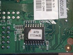
Sticker on the flash IC showing the firmware version.
Klicken Sie hier, um diesen Beitrag zu bewerten!
[Total: 0 Durchschnitt: 0]